
Laser processing, in-plane micro-supercapacitor (MSC) , porous conductive carbon interdigitated electrode, reduced graphene oxide electrode,
rechargeable magnesium battery, wearable UHF-band RFID tag, UHF-band RFID tag sensors
Our mission
LP&D Laboratory (LP&D Laboratory, Laser Processing & Devices Laboratory) aims to contribute to society through technology innovation and manufacturing based on open-source methodologies. We will openly share our knowledge, experience, technology, intellectual property, and know-how gained through research and development at universities and companies, and will challenge innovation through the provision of prototype samples and collaboration among different fields and industries.
Element technology
Our elemental technologies are mainly related to laser processing, which is a technology for converting and processing materials by irradiating and scanning laser beams. Laser processing is an on-demand manufacturing technology that gives a shape based on computer-generated designs, and is suitable for the manufacturing of a prototyping device custom manufacturing by small-scale business. It is also a clean technology that does not generate waste fluid and has a low environmental impact.
Creation of new materials by interaction of laser beam with materials
Porous conductive carbon
Laser processing enables laser direct writing of fine patterns by focusing and scanning a laser beam. This technique is often compared to fine patterning by photolithography. In laser processing, a high-energy laser beam is focused onto a material with a high spatial resolution. This causes a unique interaction between the laser beam and the material, which cannot occur in photolithography. This enables 3D texturing of the material surface and formation of a 3D structure with a high aspect ratio by laser ablation, which are difficult to achieve by photolithography.
We have been developing devices such as in-plane micro supercapacitors (electric double layer capacitors) and sensors by using interdigitated electrodes of porous conductive carbon obtained by laser direct writing. A large surface area due to their porous structures is advantageous to the devices. Porous conductive carbon layers also have reactive functional groups, which as a deferent feature from metal electrodes with flat surfaces. We can provide prototype samples and custom-made electrodes made of porous conductive carbon layers. The examples are shown on the R&D 1 and 2 pages.

SEM image of porous conductive carbon.
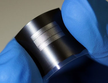
Interdigitated electrode consisting of a porous
conductive carbon layer.
On-demand manufacturing technology
Image designed on the computer takes shape instantly
Tact time (the time required to produce a single product) is often an issue when comparing laser processing and photolithography. Photolithography is better suited for mass production of a same product. On the other hand, laser processing technology excels in manufacturing products that can be designed by computer and immediately formed into various shapes. Comparing their takt time, photolithography is superior for mass production of identical products, while laser processing, which does not require masks or expensive equipment for custom design of various shapes, is superior in terms of R&D efficiency.
As an example of device development for which laser processing is suitable, various UHF RFID tag sensors that we have researched and developed are shown in R&D pages 3, 4, 5, and 6. Because UHF RFID tags are very sensitive to the influence of the surrounding environment, the results of electromagnetic field simulation do not always match the characteristics of the actual prototype RFID tag. In particular, for UHF RFID tag sensors that are to be attached not to free space (in the air) but to high-k dielectric materials such as the human body or to metal surfaces, it is essential to conduct research and development by repeatedly making prototypes of tags of various shapes and measuring the actual tag characteristics.
We offer on-demand manufacturing technology using laser processing to bring ideas on the computer to shapes instantly.

UHF RFID Tag Sensor Design designed on computer and the electro-magnetic field simulation.

Prototype wearable UHF RFID tag sensor with various shapes
by laser processing.
We develop devices such as flexible and wearable in-plane micro supercapacitors, rechargeable batteries carbon microelectrode sensors based on a porous conductive carbon prepared by laser processing, and UHF RFID tag sensors, and the on-demand manufacturing technology by laser processing. We also provide technical information, prototype, and custom products, and offer equipment and technical information related to laser processing.